Launch of three new systems — NUCLEUS, ORCAS and SUNBIRD — to support wafer level / panel level packaging market
Hong Kong and Singapore, 21 December 2015: ASM Pacific Technology Limited (“ASMPT”), a world leader in the supply of semiconductor assembly and packaging equipment and materials, as well as surface mount technology applications, announced its broad portfolio of wafer level and panel level technological capabilities will enable customers/manufacturers to meet the industry’s demand for smaller, faster and powerful devices.
Wafer level packaging (“WLP”) is one of the latest packaging trends in microelectronics, driven by demand for devices to have thinner, smaller form-factor and high performance with excellent electrical and thermal properties. According to market research and strategy consulting firm Yole Developpement, the market would reach more than $150 million in 2014 and a CAGR of 30% for the next five years is expected, driven by mobile applications and the need of very thin packages for high I/O devices .
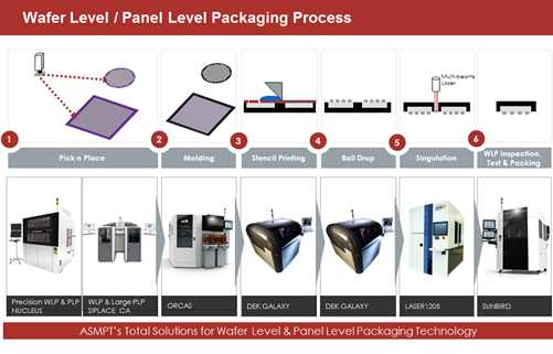
Built on the company’s rich R&D, ASMPT’s total solutions for wafer level and panel level packaging technologies from pick & place to large format mold, stencil print, ball drop, singulation and test & finish will help manufacturers/customers to meet the industry’s demand for advanced semiconductor chips with greater functionality.
Mr Nelson Fan, Vice President of Business Development of Advanced Packaging Technology for Back-end Equipment Segment of ASMPT said: “In recent years, ASMPT has been building up and strengthening our capabilities in advanced packaging applications. To further expand our portfolio in advanced packaging applications, we invested in laser dicing and grooving wafer business and MIS substrates in early 2014 and October 2015 respectively. With our comprehensive suite of advanced packaging solutions, we are well-positioned to work with customers to develop the solutions they need to meet the industry’s demanding requirements — to increase performance while addressing the need for more functionalities and reduced cost. Our latest innovations such as NUCLEUS, ORCAS and SUNBIRD will further aid customers to accelerate the speed-to-market and boost their competitiveness.”
ASMPT’s complete portfolio of wafer level and panel level packaging technologies include:
Pick & Place Process
• The NUCLEUS is one of the ASMPT’s latest advanced packaging solutions for precision placement. It is designed to address different fan-out assembly approaches such as die-up or die-down with local and/or global alignment modes. The NUCLEUS is capable of fully automated multi-die bond processing with its large work holder for 12” wafer substrate and up to 330 x 330mm panel substrate, making it ideal for wafer level packaging and panel level packaging. Apart from high throughput, the NUCLEUS also provides high bonding accuracy with a XY placement accuracy of less than 2.5µm at 3σ. The NUCLEUS comes with an optional feature which provides an additional processing capability for high bond force and bond temperature catering to a specific process requirement of high-end device application.
• The SIPLACE CA is the world’s first placement platform that combines multi bare-die placement directly from the wafer and classic SMT placement in a single machine and a single production process. Perfect for high speed large panel level packaging, it delivers maximum performance and capability. When equipped with the SIPLACE Speedstar CP20 head, the SIPLACE CA is able to place up to 42,000 flip-chips or 28,000 die-attach components per hour in sizes ranging from 03015” (0.3 x 0.15mm) up to 6 x 6mm with an accuracy of ±10µm / 3σ for eWLB process and components up to 27 x 27mm with ±25µm / 3σ.
Molding Process
The ORCAS is a new and robust encapsulation system with configurable molding direction and pressing capabilities which gives it unprecedented flexibility in producing fan-out and fan-in wafer level packages as well as panel level packages. It can also encapsulate different types and sizes of substrates, as well as handles both liquid and granular encapsulation which can be incorporated within the same system. The ORCAS delivers a high co-planarity accuracy of ±20μm with its robotic handler providing the required stability. It can be configured for multiple press usage.
Stencil Printing & Ball Placement Processes
The DEK Galaxy is a high throughput and high accuracy system with in-line capability for highest automation. It is capable to deliver a high throughput with an alignment capability of minimum 2Cpk @ ±12.5µm. The DEK Galaxy is a modular system and the printer can be used for other material depositing processes as well.
One of the material deposition processes which includes depositing solder spheres at substrate- and wafer-levels, allows placement of solder balls as small as 200µm and up to 1.2mm on the same machine. It meets the industry’s speed and accuracy requirements, delivering greater than 99.99% placement yield at a high throughput and with an intelligent detection system for assurance of process.
Singulation Process
The LASER1205 multi-beam dicing system has the ability to dice (Si among others) substrate material of thickness from 10μm up to 250μm as well as Die Attach Film (DAF) or Film Over Wire (FOW) on which the substrate is laminated, as well as mold compound structures (WLCSP and FOWLP). In addition to small Heat Affected Zone (HAZ) (typically less than 2μm) and narrow dicing width (12μm for 100μm thickness), the LASER1205 in the case of molded compound structures can achieve a dicing width of 16μm for a 400μm thick mold compound structure. It has high position accuracy and a reproducibility of less than 1.5μm. The LASER1205 also has features like ultra-short index time, kerf check ‘on the fly’, dual cassette stations, and dual coat and clean stations which ensure high UPH that is typically faster than competitors by 50%.
WLP Inspection, Test and Packing Process
The SUNBIRD, a new innovation from ASMPT, is a sophisticated system providing total solution on sorting, six-side inspection and flexibility for an individual unit testing and laser marking. The system is equipped with iTechnology features to provide the user an intelligent machine of high stability, good yield and reliable die handling at high speed. Applications include wafer level packages / dice inspection comprising micro crack inspection at six sides and sorting according to wafer mapping generated from the upstream processes.
ASMPT will showcase some of the above leading innovations on wafer level and panel level technologies at the coming SEMICON Korea 2016 event which will be held in Seoul from 27 January to 29 January 2016.
– END –
About ASM Pacific Technology Limited
ASM Pacific Technology Limited (“ASMPT”) (HKG: 0522), as a global technology and market leader, develops and provides leading edge solutions and materials for semiconductor assembly and packaging industries, as well as surface mount technology solutions in a wide range of end-user markets including electronics, mobile communications, automotive, industrial, LED and solar energy. ASMPT consistently invests in R&D to provide customers with innovative and cost-efficient solutions and systems that help them to achieve higher productivity, greater reliability and enhanced quality.
Listed on the Hong Kong Stock Exchange in 1989, ASMPT is currently one of the constituent stocks on the Hang Seng HK Mid-cap Index under the Hang Seng Composite Index, the Hang Seng Information Technology Industry Index, the Hang Seng Hong Kong 35 Index and the Hang Seng Global Composite Index. To learn more about ASMPT, please visit www.asmpacific.com.
~~~~~~~~~~