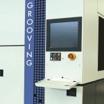
UV Grooving
Multi beam Matrix laser grooving process allows full removal (grooving) of the top layers (Low-K, Metals and passivation, etc). The multi beam matrix grooving process creates a U-Shape groove profile with consistent industry standard quality (low burr, no chipping, smooth groove profile). The unique slider concept (wafer stepper concept) allows high accuracy and reproducibility. Together with unique and patented “kerf check on the fly” the customer has continuous process control:
Key Features:
- Large variety of grooving widths. Ranging from 10um up to 100um or more due to wide selection of multi beam matrix configurations.
- Extremely high position and grooving accuracy and repro (< ± 1um)
- High UPH (typically 50% faster than competition) due to system concept design focused on laser material processing:
- ultra short index time
- Kerf check on the fly
- Dual cassette stations
- Dual coat and clean stations
Summary Key Points:
• Unique Multi beam technology
• Active focus control to compensate for wafer thickness variations
• Planar motion system & active mounts for vibration compensation provide extremely high speed & accuracy
• Remote control and diagnostics for on the spot process support and faster service support
• 2 individual cassette stations to eliminate machine idle time
• Priority wafer or wafer inspection port for maximum flexibility and control
• (Multiple) Integrated coating/cleaning stations to maximize dicing productivity & flexibility
• Automatic beam splitting exchange for multiple applications
• Pre-alignment and contour station to enable maximum productivity
• Multi-Project Wafer (MPW) and broken wafer dicing capability for tool flexibility & higher wafer yield
• ‘‘ On the fly’’ kerf check for grooving processes with no throughput loss
• Automatic Spot to Lane (S2L) sensor
• Secs Gem compatible
• Intuitive Graphical User Interface
Applications:
• Low-K grooving
• Logic IC
• LCD drivers
• Micro processors
• Memory
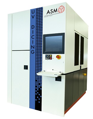
UV Dicing:
ASMPT is the inventor of multi beam semiconductor dicing. With this experience we have developed a V-DOE dicing technology which allows full cut dicing of Low-K (thin) Si wafers including DAF or FOW while achieving high die strength (450-500Mpa) with a good quality and low CoO. The V-DOE process allows customers to dice through the full stack of materials using a single process step. No complicated and costly process flows required such as with DBG or other Hybrid dicing technologies. The unique slider concept (wafer stepper concept) allows high accuracy and reproducibility.
Key Features:
- Ability to dice substrate material as well as DAF or FOW. Thickness ranging from 10um up to 200um.
- High position accuracy and repro (< ± 1um)
- Narrow dicing width (< 12um for 100um thickness)
- Small HAZ (< 2um for 100um thickness)
- High UPH (typically 50% faster than competition) due to system concept design focused on laser material processing:
o ultra short index time
o Dual cassette stations
o Dual coat and clean stations
Summary Key Points:
• Unique Multi beam technology
• Active focus control to compensate for wafer thickness variations
• Planar motion system & active mounts for vibration compensation provide extremely high speed & accuracy
• Remote control and diagnostics for on the spot process support and faster service support
• 2 individual cassette stations to eliminate machine idle time
• Priority wafer or wafer inspection port for maximum flexibility and control
• (Multiple) Integrated coating/cleaning stations to maximize dicing productivity & flexibility
• Automatic beam splitting exchange for multiple applications
• Pre-alignment and contour station to enable maximum productivity
• Multi-Project Wafer (MPW) and broken wafer dicing capability for tool flexibility & higher wafer yield
• Secs Gem compatible
• Intuitive Graphical User Interface
Applications:
• RFIC
• HB-LED
• Memory (NAND & DRAM)
• Power
• LCD drivers
• Micro processors
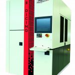
IR Dicing:
ASMPT is the inventor of multi beam semiconductor dicing. With more than 20 years of multi beam laser process experience in high volume manufacturing many billions of parts have been processed. Utilizing the strength of the multi beam process, low power per beam but using many beam to allow high material removal rate with a small (<3um) heat affected zone. The unique slider concept (wafer stepper concept) allows high accuracy and reproducibility. The IR multi beam laser process has proven its value in semiconductor wafer singulations and enabled the ongoing trend of thinner (more fragile) devices and shrinking the dicing street resulting in more die per wafer.
Key Features:
- Typical dicing thickness ranging from 10um up to 250um.
- High position accuracy and repro (< ± 1.5um)
- Narrow dicing width (< 17um for 100um thickness)
- Small HAZ (< 2um for 100um thickness)
- High UPH (typically 50% faster than competition) due to system concept design focused on laser material processing:
-
- ultra short index time
- Dual cassette stations
- Dual coat and clean stations
- Secs Gem control and remote support control functionality
- Pre alignment station to enable maximum productivity
- Broken wafer and Multi Project Wafer software functionality
- Intuitive Graphical User Interface
Applications:
- RFIC
- HB-LED
- Discretes; Transistor & Diodes
- Power